Selection of NIR devices
Did you know it’s now possible to PRINT infrared detectors smaller than 10 micrometers? 😮😮
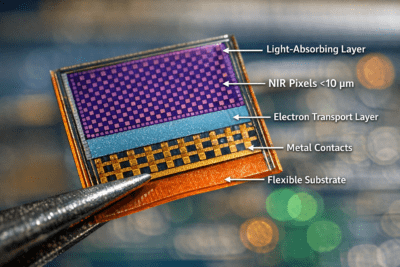
In a recent study by Zhixuan Zhao and Ran An at the National University of Singapore, the team developed pixels using semiconductor nanocrystals, printed layer by layer on a flexible substrate, combining a light‑absorbing layer, an electron transport layer, and metal contacts.
Each pixel acts as a sensor: when NIR light hits it, photons transfer their energy to electrons in the absorbing layer, exciting them and freeing them to move. This movement of electrons generates an electrical current, which is the signal used to detect the light.
The material they printed absorbs optimally between 1,000 and 1,500 nm, depending on the nanocrystal bandgap. The designed detector has maximum sensitivity in that window. Covering the full NIR range would require combining multiple materials or nanocrystals with different bandgaps, highlighting interesting opportunities for future developments.
Read the full study here: https://lnkd.in/eHvP3zM3
Do you work with NIR instruments in your laboratory? At Vibralytics, we can help you choose the right device for your application and guide you in implementing it effectively.